Dead, Stuck and Bright Pixels: Definitions and Acceptance Limits
Dead, stuck and bright pixels explained: how each state differs, how the classes are counted and how acceptance limits are written for a product. | Target URL: https://blog.cdtech-lcd.com/dead-stuck-bright-pixel-spec/
Pixel defects are the most contractible display defect there is: each state is defined, each has a counting rule and each can be inspected in minutes. The difficulty is not detection but agreement – which class a pixel belongs to, how clusters are counted, and what limit suits the product. Getting that agreement in writing before the first shipment removes the most common cosmetic dispute in display supply.
Part of the Quality, Testing & Compliance guide — 33 articles on defect classes, inspection, qualification and certification.
The three states, defined
Dark, coloured and permanently lit.
A dead pixel stays black because it never opens: the driving transistor or the cell itself has failed, so no light passes. A stuck pixel is permanently at one state, usually showing a fixed colour such as red, green or blue because one subpixel is driven continuously. A bright pixel is a subpixel that stays on at full or partial intensity, appearing as a white or coloured dot on a dark background. Because the three have different mechanisms, a scanner or a human can separate them with two test patterns.
The distinction matters for acceptance because some standards count them differently, and because a cluster of adjacent failures suggests a different cause from isolated ones.
How a pixel fails
Three failure sites, three signatures.
Failures occur in the thin-film transistor that switches the pixel, in the cell itself – a short, a particle, a spacer problem – or in the driver circuitry that supplies the row or column. Transistor and cell failures usually affect a single pixel or subpixel; driver failures affect a line or a region, which places them in the line-defect category rather than the pixel category. A particle trapped in the cell can produce a bright or dark spot depending on where it disturbs the field, which is one reason a bright pixel is not automatically classified as an electrical fault.
For a buyer, the useful question is whether the defect is isolated or systematic: one pixel in a thousand units is a yield matter, while the same pixel position failing repeatedly points at a process or mask issue.
Single defects, clusters and lines
Counting rules change with geometry.
A single defective pixel is counted individually. Two or more adjacent defective pixels form a cluster, and most standards treat a cluster as more serious than the same number of isolated defects, because it is more visible and more likely to grow. A line or a region is a functional defect and normally a rejection regardless of count. The acceptance standard should therefore define the cluster size threshold and treat clusters and lines under separate rules from isolated pixels.
That structure prevents the common argument in which a supplier adds up isolated and adjacent defects and claims the total is within an overall limit.
Pixel defect classes in practice
The ISO 9241-307 family is the usual reference.
The standard defines defect types – dark, bright and coloured subpixel or pixel failures – and sets out classes that permit different numbers of each type. Class II is the one most often quoted in commercial display supply; stricter classes are used where a single visible defect is unacceptable. The important practical point is that the class defines both the type and the count, so a specification that names a class without stating which defects it covers is incomplete. CDTech’s ISO 9241-307 explainer sets out the definitions.
Where a product is used for medical interpretation or inspection, the customer usually specifies a stricter class or a zero-defect-in-the-centre rule rather than relying on the default.
How to inspect for pixel defects
Two patterns, controlled light and a defined distance.
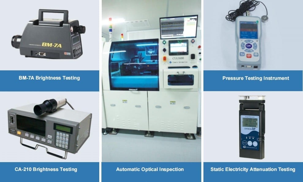
Inspection uses a full-white pattern to reveal dead pixels and a full-black or dark pattern to reveal bright ones, with the display at the brightness setting used in service. The light in the room should be low enough that a bright pixel is obvious and the viewing distance defined so that operators apply the same threshold; a magnifier is used to confirm classification, not to find defects. Because a bright pixel on a dark background is easier to see than a dark pixel on white, the same defect count can look different in the two patterns, which is why both are always used.
Automated optical inspection adds repeatability, and its defect categories should map onto the acceptance classes so that factory data and incoming data are comparable.
Writing acceptance limits
Type, count, zone and cluster rule.
| Element | What to state |
|---|---|
| Defect types | Dark, bright and coloured, defined per subpixel and per pixel |
| Counts | Maximum of each type per unit, and per zone where the product allows |
| Zones | Centre, general area and edge, with stricter limits in the centre |
| Clusters | Maximum cluster size and whether adjacent defects count as one |
| Lines and regions | Zero tolerance, as a functional defect |
| Inspection | Patterns, brightness setting, illumination, distance and magnification |
Where the product has a viewing-critical area – a numeric readout, a waveform – the standard can define a protected zone with a stricter limit, which is often more useful than tightening the whole screen.
Limits by application
The acceptable count follows the consequence.
A signage panel read at a distance tolerates isolated defects that a bench instrument would not, because they are invisible at the viewing distance. A medical or inspection display usually specifies a stricter class and a clean centre zone, since a defect in the image area can be mistaken for clinical or measured information. A consumer-facing kiosk sits between the two: defects in the interactive area are noticed, defects in a border hidden by a bezel are not.
Expressing the requirement in terms of visibility at the working distance is often easier to justify than picking a class number, and it can be translated into a class afterwards.
Incoming inspection and sampling
Sample size follows the cost of a miss.
Where a bright pixel in the centre would cause a field return, inspecting that characteristic on every unit or with a tight plan is justified; where defects are cosmetic and the supplier’s process is stable, sampling with a defined acceptance number is enough. Recording the type, count and position per lot turns the inspection into trend data, which is what reveals a process drift before it becomes a rejected batch. CDTech’s notes on what to test when LCDs arrive cover the receiving routine.
Rejected units should be preserved for the supplier’s analysis, since the position and type are the evidence that identifies the cause.
What to ask a supplier about pixel defects
Five questions that make the claim checkable.
- Which class is quoted, and which defect types it covers.
- Whether inspection is manual or automated, and at what threshold.
- What the historical defect rate is per lot, by type.
- Whether adjacent defects are counted individually or as clusters.
- What happens when a lot exceeds the limit – sorting, replacement or credit.
Workmanship and inspection expectations for the assembly are published by bodies such as IPC, verification scopes by laboratories such as Intertek, and colour and appearance definitions by the CIE. Certificate scope for the factory can be checked as described by the International Accreditation Forum, and panel defect trends are reported by research firms such as TrendForce.
Prevention and process control
Most pixel defects are yield, and yield follows process control.
Transistor and cell defects originate at the panel fab and are managed by the panel maker’s yield programme, which the module supplier can only select for and screen. Driver and connection defects are more often module-level: COG bonding parameters, FPC bonding, static control during handling and ESD protection during assembly all affect the rate. That split explains why a change in defect rate sometimes appears without any change in the panel supply, and why the analysis should always state which type increased.
Related process material is collected in CDTech’s quality assurance and factory compliance pages and at the display and touch solutions centre.
FAQ
What is the difference between a dead pixel and a stuck pixel?
A dead pixel stays black because it never opens, so no light passes. A stuck pixel is permanently at one state, usually showing a fixed colour because a single subpixel is driven continuously. Both are inspected with a white and a black pattern, and they are counted as different defect types.
How many dead pixels are acceptable?
It depends on the class the product specifies and the viewing distance. The ISO 9241-307 classes set permitted counts by defect type, and products with critical content usually specify a stricter class or a clean centre zone rather than relying on the default. The limit should be written into the acceptance standard.
Is a cluster of defective pixels worse than the same number of separate ones?
Yes in most standards: adjacent defects are more visible and more likely to grow, so clusters are counted as a separate category with their own limit. A specification that only caps the total count can be satisfied by a cluster that a customer would reject.
Can pixel defects be repaired?
Not in the field. A defective pixel is a transistor, cell or connection failure inside the panel or its bonding, so the unit is either accepted under the class limit or rejected. Field repair of individual pixels is not a practical option for industrial modules.
Next step
Send the application, viewing distance and the class you intend to specify to CDTech; the reply will state the achievable defect level and propose acceptance wording that matches the product.
Contact sales@cdtech-lcd.com or use the contact page.
Related articles
 Second-Source Qualification for Display Modules Without Doubling Your Inventory RiskQuality, Testing & ComplianceIncoming Inspection for Display Modules: What to Check and How OftenQuality, Testing & ComplianceEMC Certification for Display Products: Passing the First TimeQuality, Testing & ComplianceScreen Damage Modes: Distinguishing Production Defects From Field DamageQuality, Testing & Compliance