How Does ESD Protection Make Displays More Reliable?
ESD protection makes industrial displays more reliable by intercepting high-voltage electrostatic pulses before they reach touch controllers, display drivers, or interface ICs. A robust design combines low-capacitance TVS protection, short discharge paths, controlled grounding,…
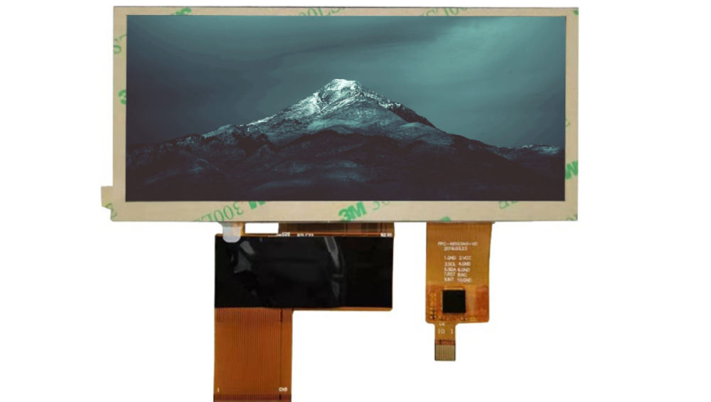
ESD protection makes industrial displays more reliable by intercepting high-voltage electrostatic pulses before they reach touch controllers, display drivers, or interface ICs. A robust design combines low-capacitance TVS protection, short discharge paths, controlled grounding, filtering, and enclosure-level shielding. For exposed industrial terminals, protection must be engineered into the FPC, PCB, touch panel, connector, and chassis as one coordinated system.
What Makes ESD Dangerous to Industrial LCD Displays?
Electrostatic discharge becomes dangerous when accumulated charge suddenly finds a path through a display assembly. The pulse may last only nanoseconds, yet its voltage can reach several kilovolts. Instead of immediately destroying the LCD itself, ESD often attacks touch controllers, interface ICs, power rails, FPC connections, or display-driver circuitry.
This distinction matters in failure analysis.
When an industrial screen suddenly turns white after an operator touches the housing, the first conclusion is often “LCD failure.” On the production floor, however, we frequently approach this differently.
The LCD glass may still be perfectly functional.
A typical discharge path can look like this:
Operator → bezel → touch-panel edge → FPC → controller/driver IC → PCB ground
Depending on where the energy enters, several symptoms can appear:
- temporary touch freezing;
- random or “ghost” touch coordinates;
- display flickering;
- horizontal or vertical corruption;
- white screen until power cycling;
- MCU or touch-controller reset;
- permanent communication failure;
- latent semiconductor damage that appears weeks later.
The last category is particularly troublesome.
A severe ESD event can cause immediate electrical overstress and catastrophic failure. Lower-energy repetitive events may instead weaken protection structures inside an IC without producing an obvious factory-test failure.
This is one reason industrial display reliability cannot be judged only by whether a module powers on after an ESD test.
At CDTech, display protection therefore needs to be considered from the external touch surface all the way to the host-side electrical interface.
Why Are Handheld Industrial Displays Especially Vulnerable?
Handheld terminals combine frequent human contact, plastic housings, exposed seams, charging interfaces, touch surfaces, and mobile operation. Dry air and friction from clothing, gloves, packaging materials, seats, conveyor systems, or synthetic flooring can repeatedly charge the operator before the display is touched.
Consider a warehouse scanner.
An operator walks across a dry floor, removes a handheld terminal from a synthetic holster, and touches the screen hundreds of times per shift. Charge generation is not a laboratory anomaly—it becomes part of the normal operating environment.
The situation becomes more difficult when:
The enclosure is mostly plastic.
Plastic provides fewer predictable discharge paths than a well-designed conductive enclosure.
The display is close to the housing edge.
A discharge around the bezel may couple directly into touch-panel electrodes or the display FPC.
The touch panel has a large exposed area.
A capacitive touchscreen effectively creates a substantial coupling surface above sensitive electronics.
Long FPCs are used.
The flexible cable can become part of the coupling path rather than merely an electrical interconnect.
Ground architecture is weak.
ESD energy reaching signal ground can cause local ground potential to rise rapidly.
In our production experience, this is why replacing a failed touch controller with a supposedly “more robust” controller does not necessarily solve the underlying problem. If the discharge route remains unchanged, the new component is still standing in the same electrical firing line.
The engineering objective should therefore be:
Do not ask the IC to absorb the ESD event. Give the ESD current an easier route around it.
How Does a TVS Protection Circuit Defend a Display?
A TVS protection circuit provides a fast, low-impedance path for transient energy so the voltage presented to sensitive display electronics is limited. For exposed FPC and connector signals, carefully selected unidirectional or bidirectional TVS devices can protect touch, control, power, and communication lines without disturbing normal operation.
A simplified protection topology is:
External/FPC Input → TVS Array → Optional Filter → Display Circuit
with the TVS discharge route connected through a deliberately low-inductance ground path.
For suitable signal lines, CDTech can incorporate a bidirectional TVS array close to the FPC input region rather than positioning the protection device deep inside the PCB.
That physical placement matters enormously.
A TVS device located 30–40 mm away from the entry point may look perfectly correct on the schematic. During a nanosecond-scale transient, however, the copper between the connector and TVS has parasitic inductance.
A rough relationship is:
V = L × di/dt
When current changes extremely rapidly, even a small inductance can generate significant additional voltage.
This creates one of the most important lessons we see in real hardware development:
A correct protection component with poor PCB placement can perform worse than a modest protection component with excellent placement.
Selection also requires more than checking the package voltage.
| Parameter | Engineering Question | Display Design Impact |
|---|---|---|
| Working voltage | Is normal signal voltage safely below VRWM? | Prevents unwanted conduction |
| Clamping voltage | How high does the protected node rise? | Determines stress reaching the IC |
| Capacitance | Will protection load the signal? | Critical for high-speed interfaces |
| Polarity | Is bidirectional behavior required? | Depends on signal characteristics |
| Pulse capability | Can the device survive expected events? | Affects repeated-event reliability |
| Package/layout | Can it sit directly at the entry point? | Influences parasitic inductance |
Low capacitance becomes especially important for high-speed display interfaces. Simply installing a large TVS diode everywhere can protect against transients while simultaneously degrading the eye diagram.
Protection and signal integrity must therefore be engineered together.
How Should TVS Diodes and Ground Rings Be Laid Out?
TVS devices should be placed as close as practical to the ESD entry point, with short traces and a low-inductance return to chassis or an appropriate ground plane. A GND ring or perimeter discharge structure can then redirect edge-coupled energy away from touch controllers, display-driver circuits, and sensitive high-speed traces.
Think of the PCB as terrain during a flash flood.
The ESD pulse will follow available impedance paths. The designer’s job is to build a drainage channel before the flood reaches the electronics.
A useful topology is:
ESD Entry Point
↓
TVS Clamp
↓
Short/Wide Discharge Path
↓
GND Ring / Ground Plane / Chassis Path
while the protected signal continues toward the display electronics.
One mistake we regularly watch for during layout review is placing the TVS beside the signal trace but connecting it through a long branch.
Electrically, the schematic says the TVS is connected.
Physically, the ESD pulse encounters the branch inductance before reaching it.
We instead prefer a layout where the transient meets the protection structure immediately after entering the board.
A perimeter GND ring can provide another defensive layer. Around vulnerable FPC or PCB regions, the grounded copper structure creates a preferred discharge path before energy couples deeper into the circuitry.
But the ring cannot simply be decorative copper.
Its effectiveness depends on:
- continuity;
- connection impedance;
- via placement;
- relationship to chassis ground;
- distance from sensitive traces;
- enclosure construction;
- cable and shield grounding.
The return path is often more important than engineers initially expect.
If TVS current is dumped into a thin signal-ground trace shared with a touch controller, the protection event itself can create ground bounce. The IC may survive electrically yet reset because its reference potential moves abruptly.
That is protection without functional immunity.
Which Display Signals Need Different ESD Protection Strategies?
Not every display signal should receive the same TVS device or filter. Low-speed touch, GPIO, reset, I²C, USB, LVDS, MIPI, HDMI, and power lines have different voltage, bandwidth, impedance, and capacitance requirements. High-speed differential interfaces generally demand substantially lower-capacitance protection than slow control or power circuits.
This is where “add TVS protection” becomes an incomplete specification.
Consider four common groups.
Touch and low-speed control lines
I²C, interrupt and reset signals usually tolerate more protection capacitance than RF-like high-speed display links. These are often practical locations for compact multi-channel arrays.
Power rails
Power-line protection must be selected around normal rail voltage, expected transient energy, clamping behavior, and downstream component limits. A tiny data-line protection array should not automatically be treated as equivalent to power-rail protection.
LVDS interfaces
LVDS depends on differential impedance and signal quality. Excessive capacitance, asymmetric routing, or poor component placement can distort edges and increase jitter.
MIPI and other very high-speed links
Here the protection device itself becomes part of the transmission channel. Ultra-low-capacitance devices and carefully controlled differential routing are required.
| Interface | Main ESD Design Concern | Common Engineering Priority |
|---|---|---|
| I²C / GPIO | Controller exposure | Strong clamping |
| Touch signals | Large coupling surface | Multi-line protection |
| Power | Higher transient energy | Clamp capability |
| USB | Data integrity | Low capacitance |
| LVDS | Differential balance | Low capacitance + symmetry |
| MIPI | Very high bandwidth | Ultra-low capacitance |
| HDMI | Multiple high-speed channels | ESD protection + signal integrity |
This is why CDTech evaluates protection architecture together with the selected LCD interface and touch solution rather than treating ESD circuitry as a universal add-on.
What Does a Display Noise Filter Add Beyond TVS Protection?
A display noise filter addresses disturbances that a TVS diode alone cannot solve. TVS devices primarily clamp fast transient voltages, while resistors, capacitors, ferrites, and common-mode filters can suppress conducted or coupled interference. The correct combination depends on whether the affected line carries DC power, low-speed control, touch signals, or high-speed differential data.
This distinction frequently solves confusing field failures.
Suppose a touch panel resets during an ESD event even though the TVS diode prevents permanent damage.
The problem may now be functional disturbance rather than destructive overstress.
We may investigate:
- transient coupling into the touch interrupt line;
- noise entering the reset pin;
- temporary power-rail disturbance;
- common-mode energy on a cable;
- ground bounce around the controller;
- coupling between protected and unprotected traces.
For slow signals, small series resistance combined with carefully chosen capacitance may help reduce transient energy reaching the controller.
For high-speed differential links, that approach cannot be copied blindly. Excessive capacitance can destroy bandwidth or differential balance. A common-mode filter designed for the intended frequency range may be more appropriate.
One factory-floor lesson is particularly important:
Do not solve an ESD reset by adding capacitors randomly until the prototype passes.
That can mask the mechanism while introducing slower rise times, boot problems, communication errors, or temperature-dependent instability.
First determine where the transient enters and which node actually fails.
Then filter that path deliberately.
How Can ESD Failures Be Diagnosed Before Mass Production?
ESD failures should be diagnosed by testing accessible surfaces, bezel edges, connectors, FPC regions, housing seams, and nearby conductive structures while monitoring display power, reset, touch communication, and video signals. Engineers should distinguish permanent damage from temporary resets, communication corruption, touch malfunction, and recoverable display errors before changing the circuit.
During prototype debugging, the failure symptom is only the beginning.
For example:
Screen becomes white but backlight remains on.
That suggests a different failure path from complete power loss.
We would investigate whether the display controller stopped receiving valid video data, whether the interface lost synchronization, or whether a reset/power rail was disturbed.
Touch stops but LCD image remains normal.
The investigation moves toward the touch-controller supply, I²C communication, reset line, interrupt line, touch FPC, and grounding.
Entire terminal reboots.
Now the system power rail, MCU reset network, common ground impedance, and enclosure discharge route deserve attention.
A useful engineering sequence is:
- reproduce the failure consistently;
- identify the physical discharge location;
- classify the failure as damage, reset, corruption, or temporary malfunction;
- monitor critical rails and reset lines;
- identify the energy path;
- modify one protection variable at a time;
- repeat both polarities and relevant discharge points.
Changing three TVS devices, adding five capacitors, and modifying grounding simultaneously may produce a passing prototype—but it teaches the engineering team almost nothing about the original failure mechanism.
Controlled iteration produces designs that are easier to transfer into mass production.
Could Stronger ESD Protection Reduce Display Performance?
Yes. Over-engineered ESD protection can degrade display performance when high-capacitance TVS devices, poorly selected filters, long protection stubs, or asymmetric routing are added to high-speed signal paths. The best design achieves sufficient clamping and immunity while preserving impedance, bandwidth, differential balance, touch sensitivity, and normal operating voltage margins.
This trade-off is often overlooked during early development.
A purchasing specification might simply request “maximum ESD protection.” Electrically, maximum protection is not always the same as maximum system reliability.
Imagine placing a high-capacitance protection device on a fast differential interface.
The prototype may become harder to damage with an ESD gun, but:
- edge rates deteriorate;
- insertion loss increases;
- differential symmetry worsens;
- jitter margin shrinks;
- intermittent video errors appear.
The engineering target is therefore not the largest TVS device available.
It is the lowest practical residual transient voltage compatible with acceptable signal integrity.
The same principle applies to touchscreens.
Heavy filtering may reduce transient susceptibility but can interfere with touch-controller acquisition behavior. Changes should therefore be validated with gloves, wet-touch conditions, temperature extremes, charger noise, long cables, and the final mechanical stack whenever those conditions are relevant to the application.
That system-level approach is particularly important for industrial control, medical equipment, instrumentation, automotive electronics, and handheld terminals where the display is only one part of a much larger electrical environment.
What Are CDTech Expert Views?
CDTech Expert Views:
“One of the most expensive ESD mistakes is trying to fix the problem only by changing the TVS part number. In display projects, we first ask where the current enters and where it returns. A high-performance TVS connected through a long trace or poor ground path can still allow the touch controller to reset. We have also seen engineers add excessive capacitance to suppress ESD symptoms and then create signal-integrity problems. The more reliable approach is coordinated protection: enclosure discharge path, FPC entry protection, short TVS routing, controlled ground return, appropriate filtering, and interface-specific component selection. ESD immunity is ultimately a current-path problem, not simply a diode-selection problem.”
How Should Industrial Display ESD Protection Be Specified?
Industrial display ESD protection should be specified at system level rather than with a single voltage number. Define the intended environment, accessible discharge locations, contact and air-discharge requirements, acceptable recovery behavior, display interface, touch technology, enclosure grounding, cable configuration, and whether temporary resets or user intervention are permitted.
A useful engineering specification should answer questions such as:
- Where can an operator physically touch the finished product?
- Is the bezel metal, conductive-coated, or plastic?
- Is the LCD installed near an exposed enclosure seam?
- Which connectors are accessible?
- What display interface is used?
- Is a capacitive touch panel fitted?
- Where is chassis ground?
- How is FPC shielding terminated?
- What happens after a disturbance?
- Is automatic recovery acceptable?
- Must the display continue operating without interruption?
These questions are more useful than writing only “ESD ±8 kV” on a drawing.
For customized TFT LCD and touch-display projects, CDTech can evaluate the display module together with FPC configuration, interface requirements, touch architecture, mechanical constraints, and protection circuitry.
The company was established in Shenzhen in 2011 and operates a 10,000㎡ manufacturing facility supporting standard and customized TFT LCD, touch-screen, and HDMI display solutions. Its manufacturing and quality systems include ISO9001, ISO14001, ISO13485, and IATF16949 certifications.
For industrial customers, the practical advantage of this integrated approach is straightforward: electrical protection can be considered during display customization rather than discovered only after the customer’s final terminal enters EMC testing.
What Should Engineers Remember Before Finalizing the Design?
Reliable ESD protection requires control of the complete discharge path. Protect exposed entry points first, place TVS devices close to those points, minimize return-path inductance, prevent transient current from contaminating sensitive signal ground, and select filtering according to interface bandwidth rather than applying one circuit universally.
The most actionable rule is simple:
Design where the ESD current should go before worrying about where it might go.
For an industrial display, that means looking beyond the LCD panel.
Evaluate the touch surface, bezel, enclosure seams, FPC, connectors, TVS array, ground ring, PCB ground, chassis connection, power rails, communication interface, and host electronics as one electrical system.
A display that survives a laboratory pulse but freezes in field operation is not sufficiently protected. Likewise, a heavily protected interface that introduces intermittent video errors is not a successful design.
The target is controlled energy diversion with uninterrupted signal integrity.
For demanding handheld terminals and industrial equipment, engineering the protection topology during the LCD customization stage is usually more effective than attempting to retrofit protection after certification testing exposes a weakness.
What Are Common Questions About Display ESD Protection?
What is the difference between ESD and electrical overstress?
ESD is a very fast electrostatic transient, while electrical overstress is a broader category covering electrical conditions exceeding component limits. An ESD event can cause electrical overstress, but sustained overvoltage, incorrect power sequencing, or excessive current can also produce overstress without electrostatic discharge.
Does adding a TVS diode guarantee that an LCD will pass ESD testing?
No. TVS selection is only one part of the protection system. Placement, trace inductance, ground-return impedance, enclosure construction, connector shielding, FPC routing, filtering, and coupling into neighboring circuits can determine whether the finished product remains functional.
Should every display signal use the same TVS diode?
No. Power, GPIO, I²C, USB, LVDS, MIPI, HDMI, and touch signals have different voltage and bandwidth requirements. High-speed interfaces normally require very low-capacitance protection so that ESD suppression does not compromise signal integrity.
Why can a touchscreen freeze even when nothing is physically damaged?
The ESD pulse may disturb the controller’s supply, reset, interrupt, communication bus, or ground reference without exceeding the semiconductor’s destructive limit. The controller survives but enters an abnormal state. Improving the discharge path and filtering the affected node can often eliminate this behavior.
When should ESD protection be designed into a custom LCD module?
As early as possible. The best time is during interface, FPC, touch-panel, PCB, and enclosure definition. Waiting until final EMC testing greatly restricts placement and grounding options, making corrective changes more expensive and potentially forcing mechanical or PCB redesigns.