How Can Touch Screens Achieve ESD and EMI Immunity?
Touch screen ESD and EMI immunity depends on controlling noise at its source, blocking coupling paths, and safely diverting transient energy before it reaches the touch controller. A robust design combines low-noise LCD timing,…

Touch screen ESD and EMI immunity depends on controlling noise at its source, blocking coupling paths, and safely diverting transient energy before it reaches the touch controller. A robust design combines low-noise LCD timing, grounded FPC shielding, correctly placed TVS arrays, clean power rails, short return paths, tuned controller firmware, and system-level testing under real operating conditions.
touch tuning for noise immunity and firmware customization
What Causes EMI in Capacitive Touch Screens?
Capacitive touch EMI occurs when electrical noise changes the tiny capacitance signals measured by the touch sensor, causing missed touches, false touches, unstable coordinates, or total touch lockup.
Projected-capacitive touch panels measure very small changes in mutual or self-capacitance. The useful touch signal can be small enough that ripple from a switching regulator, LCD VCOM transitions, LED backlight current, USB power, radio transmitters, or poorly grounded metalwork becomes part of the measured signal.
The most misleading fault is the “works with a finger, fails with a charger” complaint. In many cases, the touch sensor itself is healthy. The charger ground reference, common-mode current, or DC/DC switching frequency changes the noise environment enough to reduce the controller’s signal-to-noise margin.
Common interference paths include:
- LCD VCOM and source-driver switching noise coupling through the display stack.
- LED backlight boost-converter ripple coupling into touch FPC traces.
- Common-mode noise entering through USB, Ethernet, CAN, or external power.
- Long touch flex tails acting as receiving antennas.
- Floating metal frames, decorative conductive coatings, or unbonded backplates.
- High-energy electrostatic discharge entering through a cover lens, bezel gap, or exposed connector.
In CDTech touch display projects, noise diagnosis starts by identifying whether the disturbance is synchronous with display refresh, backlight dimming, a power converter, or an external cable event. That distinction prevents teams from using firmware filtering to hide a hardware coupling problem.
How Does LCD VCOM Noise Affect Touch?
LCD VCOM noise can interfere with capacitive touch sensing when common-electrode switching couples through the panel stack, FPC, ground return, or sensor electrodes and overlaps with the touch controller’s measurement window.
VCOM is the alternating common-electrode voltage used to prevent DC bias across LCD pixels. Its waveform is normal for the display, but its transitions can create broad-band energy. If the touch sensor, touch controller, and LCD share an uncontrolled return path, that energy can appear as a false capacitance change.
The symptoms are usually recognizable:
- Ghost touches that repeat at a fixed screen location.
- Touch failure only when the panel is enabled.
- A noisy vertical or horizontal band that follows display brightness.
- Stable touch at low brightness but poor touch at high brightness.
- Stronger false touches at certain refresh rates or display timing modes.
In production runs, we have seen a touch system pass initial bench testing with a static white image but fail when a moving high-contrast pattern was displayed. The display content changed source-driver activity and made the VCOM-related coupling easier to detect. A static test screen is therefore not a sufficient noise validation method.
The practical target is not “zero VCOM noise.” Every LCD has switching behavior. The target is to prevent the noise from reaching the touch sensing path at a level that compromises the controller’s detection margin.
Which Hardware Layout Reduces Touch Noise?
The most effective touch-noise layout keeps sensor traces short, separates them from switching and high-speed lines, uses a continuous low-impedance ground reference, and places the controller close to the touch FPC connection.
The physical layout of the FPC and host PCB is often more important than adding a stronger software filter. A filter may suppress random false events, but it cannot restore a sensing channel whose signal is continuously buried under display or power noise.
A practical touch-system topology is:
Cover Lens
   │
Touch Sensor ITO Pattern
   │
Shield Layer / Mesh Ground
   │
Touch FPC ── TVS Array ── Series Damping ── Touch Controller
                    │
              Chassis Ground
                    │
         Low-Impedance System Ground
For a custom FPC, place the TVS protection array near the point where exposed touch lines enter the protected electronics area. The ESD current must be diverted before it travels down a long trace toward the touch controller.
The touch controller should sit close to the FPC connector whenever architecture allows. A 30–50 mm unshielded trace may be manageable in a quiet product, but in a vehicle or industrial HMI, that same trace can become an antenna near a backlight boost circuit, display link, or RF cable.
| Layout element | Preferred implementation | Failure when omitted |
|---|---|---|
| Ground reference | Continuous ground plane beneath controller and interface traces | Unstable baseline and increased common-mode noise |
| FPC shield | Grounded mesh or conductive layer with controlled bonding points | Display or external EMI couples into sensor lines |
| TVS array | At connector entry with a short, wide return to chassis ground | ESD energy travels through protected circuitry first |
| Sensor routing | Keep away from switch nodes, LED boost inductors, MIPI/eDP lanes | Periodic ghost touches or reduced sensitivity |
| Chassis bonding | Low-impedance connection between metalwork and intended ground | Floating frame behaves as a capacitive noise antenna |
Do not route touch traces directly parallel to the switch node of a backlight boost converter. Even a short parallel section can couple a sharp switching edge into the sensor path. If separation is impossible, use grounded shielding between aggressor and victim traces, and verify the result with the final display brightness profile.
How Should a TVS Array Be Selected?
A touch-screen TVS array should have low capacitance, suitable working voltage, fast clamping behavior, and a package layout that sends ESD current directly to chassis or ground without passing through the touch controller.
TVS selection is a balance. A very robust protector with excessive capacitance can distort high-speed or sensitive touch signals. A very low-capacitance device may have insufficient surge performance for the actual system-level exposure.
For I2C and interrupt/reset lines, choose a low-capacitance multi-channel TVS array that matches the logic voltage and signal bandwidth. For touch-sensor electrode lines inside a module, protection strategy depends on controller architecture and sensor routing; adding arbitrary capacitance to sensing paths can reduce sensitivity or alter baseline calibration.
Use these selection checks:
- Confirm the maximum normal signal voltage, including overshoot.
- Ensure the TVS standoff voltage remains above the normal operating level.
- Check dynamic resistance and clamping voltage at the relevant surge current.
- Review capacitance per channel at the intended bias voltage.
- Match the channel count and pinout to minimize trace length and vias.
- Verify the device’s system-level ESD performance under the product test standard.
A common mistake is placing the TVS close to the touch IC because it “protects the chip.” Electrically, that can be too late. The ESD pulse has already traveled through the FPC, connector region, and board trace, radiating and coupling into nearby circuitry. Put the TVS at the entry point, then provide the shortest possible discharge route.
Why Does TVS Placement Matter So Much?
TVS placement determines whether ESD energy is diverted at the entry point or allowed to travel through the PCB, where it can damage components, induce resets, corrupt touch data, and radiate into nearby circuits.
A TVS diode does not eliminate ESD energy; it creates a controlled low-impedance route for that energy. The route must be physically short and electrically wide. A narrow, long ground trace adds inductance, allowing the voltage at the protected node to rise before the TVS can clamp effectively.
For touch FPC protection, follow these physical rules:
- Place TVS devices within a few millimeters of the connector whenever possible.
- Use a direct ground connection with multiple stitching vias if the TVS is on a PCB.
- Prefer short, wide traces with smooth geometry rather than long serpentine routing.
- Avoid routing protected signals underneath noisy switch-mode circuits.
- Keep the path from connector to TVS shorter than the path from connector to the touch controller.
- Direct high-energy ESD return current toward chassis ground where the enclosure architecture supports it.
In our factory-level debug work, a board that survived an air discharge at one bezel point still reset when discharged 15 mm away. The issue was not the TVS part number. The discharge current found a lower-impedance path through a frame gap and reached the controller ground before the TVS return path. Adding a controlled mesh-ground bond and reducing the return-path length solved the reset without changing the touch IC.
Can Mesh Grounding Improve EMI Immunity?
Yes. A grounded mesh layer can reduce capacitive coupling into touch electrodes by providing a controlled shielding plane, but its pattern, grounding strategy, and optical impact must be designed for the sensor and display stack.
Mesh grounding is especially useful in large-format touch displays, automotive center stacks, and industrial HMIs where the touch sensor sits close to an LCD with active switching circuits. The conductive mesh intercepts electric fields and offers a controlled reference potential between noise sources and sensing electrodes.
However, a mesh is not automatically beneficial. A poorly designed mesh can reduce touch sensitivity, create visible moiré, add optical haze, or introduce new coupling if it is floating.
Key implementation decisions include:
- Mesh pitch and line width must balance shielding effectiveness against optical visibility.
- The mesh must connect to the intended system or chassis ground with low impedance.
- Ground connection points must remain reliable through adhesive aging, vibration, and thermal cycling.
- The shield must not overlap sensing electrodes in a way that reduces usable touch signal below the controller threshold.
- The display’s polarizer orientation and pixel geometry must be checked for moiré risk.
For larger cover lenses, CDTech evaluates shielding as part of the complete stack-up: cover glass, optical adhesive, touch sensor, shield layer, LCD polarizer, backlight, FPC, and metal chassis. Testing a mesh layer by itself cannot predict final touch performance after lamination.
What Filters Work for Conducted Susceptibility?
Conducted susceptibility is best controlled by filtering noise at power and cable entry points, stabilizing touch-controller supplies, reducing common-mode current, and preventing high-frequency noise from entering the sensing reference.
Conducted noise commonly enters through DC input cables, USB charging interfaces, external adapters, and shared power rails. The goal is not to add filters everywhere. The goal is to identify the frequency and path of the disturbance, then select a component that attenuates it without destabilizing the power rail or degrading communication.
| Noise source | Effective countermeasure | Important trade-off |
|---|---|---|
| Backlight boost ripple | Local decoupling, ferrite isolation, controlled return routing | Excessive impedance can affect transient load response |
| External DC supply noise | Input LC or π filter, common-mode choke where appropriate | Resonance can worsen a narrow frequency band |
| USB common-mode noise | Common-mode choke, connector shielding, chassis bonding | Poor component choice can affect USB signal integrity |
| I2C line ringing | Series resistance and layout correction | Too much resistance can slow edges and cause timing errors |
| Touch-controller supply ripple | Dedicated low-noise LDO or filtered rail | Added heat and voltage-drop budget |
For sensitive touch-controller analog rails, a dedicated low-noise regulator or a carefully filtered branch can be worthwhile. In compact designs, do not place the regulator beside the sensor-tail connector simply because it shortens power routing. Keep switching components, inductors, and high-di/dt loops away from the sensor and touch-controller analog reference.
Firmware noise filtering should be the final layer. Raising touch thresholds may reduce ghost touches, but it also increases required touch force, degrades gloved-touch behavior, and can make edge touches feel unresponsive.
How Should ESD 15 kV Protection Be Validated?
ESD 15 kV protection must be validated on the finished product—not only on a schematic—using repeated air and contact discharges at the cover lens, bezel, connector, enclosure seams, and operating modes most likely to expose weak return paths.
A claim of “15 kV ESD protection” needs a defined test method. Air discharge, contact discharge, polarity, discharge count, test location, enclosure grounding, cable configuration, and product operating state all affect results.
For each test point, record:
- Whether touch remains functional during discharge.
- Whether false touches occur.
- Whether the display flickers, resets, or changes brightness.
- Whether Linux or Android logs a peripheral reset.
- Whether the system recovers automatically.
- Whether a latent fault appears after repeated discharges.
A product may survive a single event but fail after repeated pulses because a weak ground bond, damaged suppressor, or latched controller condition accumulates. Test both positive and negative polarity. The negative event may be more disruptive in one layout, while the positive event may expose a different clamp-path weakness.
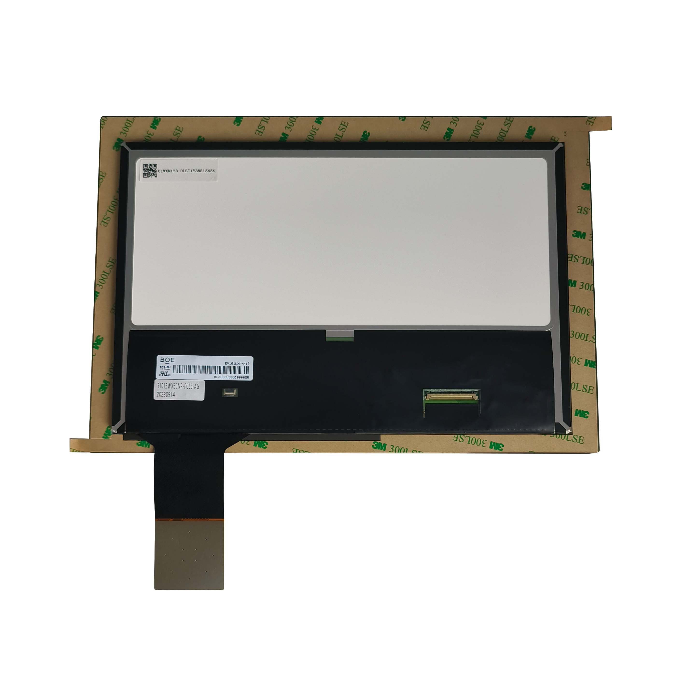
In one 10.1-inch industrial display project, the unit passed touch operation at the center of the glass but reset when discharged near the USB connector and metal frame junction. The corrective action was not increasing software debounce. It was improving connector shielding, TVS-to-chassis routing, and frame grounding continuity.
When Should Firmware Filtering Be Adjusted?
Firmware filtering should be adjusted only after electrical noise, grounding, shielding, and layout issues are controlled, because aggressive filtering can suppress false touches while making genuine touches slow, weak, or inconsistent.
Modern touch controllers can support adaptive thresholds, frequency hopping, baseline tracking, debounce intervals, water rejection, and noise-detection modes. These features are valuable, but each adds a usability trade-off.
For example:
- Increasing debounce may stop a short false event but makes fast taps less responsive.
- Raising detection thresholds can improve immunity but may harm wet-finger or glove operation.
- Strong baseline tracking can adapt to slow environmental drift but may misclassify a long stationary touch.
- Frequency hopping can avoid a fixed display-noise band but requires validation across temperature and firmware states.
At CDTech, we treat firmware settings as controlled production data, not last-minute tuning values. The final controller firmware must be tested with the approved LCD timing, cover-lens thickness, touch sensor, FPC shielding, and host power design. Changing only one of these variables can shift the noise margin.
Who Should Review the Noise-Control Design?
The display supplier, touch-controller engineer, hardware layout team, mechanical designer, power engineer, and system-validation team should review noise control together because EMI and ESD failures cross electrical, mechanical, optical, and firmware boundaries.
A touch engineer may request a mesh shield, but the mechanical team must confirm bonding reliability. The PCB team may select a TVS array, but the system team must verify its discharge path to chassis. The display team may change VCOM timing or backlight design, and the touch firmware team must recheck noise tolerance.
CDTech supports this cross-functional approach by reviewing touch stack-up, FPC routing, LCD electrical characteristics, controller selection, and system integration constraints before production release. This is particularly important for automotive, medical, and industrial interfaces where a false touch or unresponsive screen can affect operator safety and product usability.
CDTech Expert Views
“The best ESD solution is not the TVS diode with the highest published rating. It is the complete current path from the user’s discharge point to the enclosure ground. In our display programs, we first locate the actual entry path, then verify the shield bond, connector geometry, TVS placement, and return-path inductance. For EMI, we separate display-noise coupling from external conducted noise before changing firmware. That sequence avoids sacrificing touch sensitivity just to conceal an unresolved hardware issue.” — CDTech Engineering Team
What Should You Do Before Production Release?
Before release, verify touch immunity with the final LCD, touch panel, FPC, enclosure, power supply, firmware, cables, display modes, and operating temperatures—not with isolated development samples.
Use a release plan that includes:
- ESD testing at glass edges, corners, bezel gaps, connectors, seams, and exposed metal.
- Touch tests during maximum and minimum backlight operation.
- Noise evaluation with moving high-contrast display images.
- Tests with approved adapters, chargers, USB devices, and vehicle power conditions.
- Multi-touch, edge-touch, wet-touch, and gloved-touch validation where required.
- Cold boot, warm reboot, suspend/resume, and repeated power-cycle checks.
- Thermal exposure tests with post-test touch coordinate verification.
- Controlled version records for touch firmware, LCD timing, FPC revision, and PCB layout.
The most useful final metric is not merely “no reset.” It is stable, accurate, repeatable touch behavior after electrical stress, without reduced sensitivity or unacceptable latency.
FAQs
Can a TVS diode alone provide 15 kV ESD protection?
No. The TVS diode is only one part of the protection path. Connector placement, short return routing, enclosure grounding, FPC shielding, chassis bonding, and PCB layout determine whether a finished touch display can tolerate a 15 kV discharge.
Why does a touch screen create ghost touches when brightness changes?
Backlight current and LCD switching activity can inject noise into the touch sensor or its ground reference. Check VCOM coupling, backlight boost routing, FPC shielding, power-rail ripple, and the relationship between false-touch timing and brightness transitions.
Does a grounded metal frame improve touch performance?
Usually, yes. A properly grounded frame can provide a stable reference and reduce external field coupling. A floating frame is risky because it can behave like a large noise antenna and make capacitive sensing less stable.
Should I add series resistors to touch signal lines?
Small series resistors can reduce ringing and high-frequency interference on communication lines such as I2C. Their value must be selected from measured signal integrity; excessive resistance can slow edges and cause bus timing failures.
Can firmware solve all touch EMI issues?
No. Firmware can reject some noise patterns, but it cannot correct poor grounding, inadequate ESD routing, severe VCOM coupling, a noisy supply, or an unshielded FPC routed beside a switching circuit.
A durable touch-screen immunity design begins with the physical current and noise paths. Keep the display and touch reference clean, ground the mesh shield correctly, place low-capacitance TVS protection at the entry point, isolate conducted noise, and validate the finished system under realistic electrical stress. These choices protect both the touch controller and the user experience.